ZEISS Accelerates Time to Market for Advanced Semiconductor Packages with Non-destructive 3D X-ray Measurement Solution
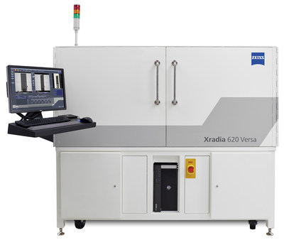
PLEASANTON, Calif., and OBERKOCHEN, Germany, Sept. 17, 2019 /PRNewswire/ — ZEISS today introduced the ZEISS Xradia 620 Versa RepScan® – a submicron-resolution, 3D non-destructive imaging solution for inspection and measurement that accelerates time to market for advanced IC packages. Utilizing 3D X-ray microscopy (XRM) with ZEISS’s revolutionary Resolution at a Distance (RaaD™) technology and sophisticated analytical software, the ZEISS Xradia 620 Versa RepScan provides rich volumetric and linear measurements of buried features in the most advanced packages that cannot be achieved with existing methods, such as physical cross-section, 2D X-ray and microCT. The result is higher-accuracy engineering data that can be used to reduce development and yield learning cycles of advanced packages.
The ZEISS Xradia 620 Versa RepScan supports design verification, product development, process optimization and quality assurance/control (QA/QC) of complex fine-pitch 3D architectures, including 2.5D interposers, high-bandwidth memory stacks with through silicon vias (TSVs) and microbumps, package-on-package interconnects, and ultra-thin memory with multiple chips in a stack.
Measurement Challenges in a 3D Packaging World
The demand for increased miniaturization and higher input/output in mobile and high-performance devices has driven an explosion of innovations that enable high-density multi-chip architectures. These designs are increasingly driving packaging interconnects into the third dimension. Measurements at critical process steps are a key enabler for the introduction and production of new and advanced technologies that have narrow process margins or are difficult to control. However, the structures in today’s advanced packages are often inaccessible or too small for measurements by non-destructive methods, such as 2D X-ray and microCT. In addition, physical cross-section lacks the ability to provide 3D volumetric data, is destructive and time-consuming, and typically provides only a small number of samples, which are often not statistically valid for improving process control.
“In this new era of 3D packaging, new approaches are needed to measure buried interconnects and other critical features with a practical throughput to enable faster time to market for new products,” stated Dr. Raj Jammy, Head of ZEISS Process Control Solutions (PCS) and Carl Zeiss SMT, Inc. “For nearly a decade, ZEISS Xradia Versa 3D XRM systems have been the standard for non-destructive failure analysis of semiconductor packages. The ZEISS Xradia 620 Versa RepScan adds a new dimension of capabilities to the industry-leading Versa platform by providing linear and volumetric measurements of critical buried features in advanced packages – enabling better processes, faster learning cycles and higher yields.”
High-resolution Non-Destructive 3D Measurements
The new ZEISS Xradia 620 Versa RepScan includes ZEISS’s proven Versa 3D XRM capability, which images and measures buried features non-destructively with submicron resolution, and extracts critical 3D information based on reconstructed 3D data sets. It can perform both linear and volumetric measurements, as well as dimensional analysis of TSVs and microbumps, solder volumes and shapes, bond line thicknesses and die warpage, 3D void analysis, and other measurements of interest with minimal need for sample preparation. The semi-automated workflow provides repeatable measurements, which ensures that no images are lost due to cross-sectioning errors, and minimizes measurement variability inherent in manual techniques.
Key features of the ZEISS Xradia 620 Versa RepScan include:
- Ability to view and measure virtually any object in any volume or plane, providing greater statistics and repeatability compared to standard cross-sections
- Proven 500 nm spatial resolution with minimum voxel size <40 nm, providing higher resolution compared to microCTs
- ZEISS’s revolutionary RaaD technology, which ensures high resolution as sample sizes increase
- Automatic loading, scanning and unloading of identical samples without the need for operator intervention, with capacity for up to 70 samples depending on part size
- Automatic transfer of scan results to a separate workstation where a variety of measurements can be executed semi-automatically
- No other automated methods exist that can provide repetitive measurement of buried features in advanced IC packages
The ZEISS Xradia 620 Versa RepScan is now available for demonstrations and shipping.
ZEISS Exhibiting at SEMICON Taiwan
ZEISS will showcase its latest microscopy products and solutions for semiconductor manufacturing – including the new ZEISS Xradia 620 Versa RepScan – at SEMICON Taiwan, to be held September 18-20 at the Nangang Exhibition Center in Taipei, Taiwan. Attendees interested in learning more can visit ZEISS at Booth M0434.
For more information on the ZEISS Xradia 620 Versa RepScan and other 3D X-ray imaging solutions from ZEISS, please visit: www.zeiss.com/pcs.
About ZEISS
ZEISS is an internationally leading technology enterprise operating in the fields of optics and optoelectronics. In the previous fiscal year, the ZEISS Group generated annual revenue totaling more than 5.8 billion euros in its four segments Industrial Quality & Research, Medical Technology, Consumer Markets and Semiconductor Manufacturing Technology (status: 30 September 2018).
For its customers, ZEISS develops, produces and distributes highly innovative solutions for industrial metrology and quality assurance, microscopy solutions for the life sciences and materials research, and medical technology solutions for diagnostics and treatment in ophthalmology and microsurgery. The name ZEISS is also synonymous with the world’s leading lithography optics, which are used by the chip industry to manufacture semiconductor components. There is global demand for trendsetting ZEISS brand products such as eyeglass lenses, camera lenses and binoculars.
With a portfolio aligned with future growth areas like digitalization, healthcare and Smart Production and a strong brand, ZEISS is shaping the future far beyond the optics and optoelectronics industries. The company’s significant, sustainable investments in research and development lay the foundation for the success and continued expansion of ZEISS’ technology and market leadership.
With approximately 30,000 employees, ZEISS is active globally in almost 50 countries with around 60 of its own sales and service companies, more than 30 production sites and around 25 development sites. Founded in 1846 in Jena, the company is headquartered in Oberkochen, Germany. The Carl Zeiss Foundation, one of the largest foundations in Germany committed to the promotion of science, is the sole owner of the holding company, Carl Zeiss AG.
Further information is available at www.zeiss.com.
Semiconductor Manufacturing Technology
With its broad product portfolio and expertise, the Semiconductor Manufacturing Technology segment of ZEISS covers a variety of key processes in the production of microchips. Its products include semiconductor manufacturing optics – notably lithography optics – as well as photomask systems and process control solutions for semiconductor manufacturing. Thanks to ZEISS technology, microchips are becoming increasingly smaller, more powerful, more energy-efficient and more affordable. The electronic applications of these ongoing enhancements enable global progress in many disciplines such as technology, electronics, communication, entertainment, mobility and energy.
Semiconductor Manufacturing Technology is headquartered in Oberkochen. Other sites include Jena, Rossdorf and Wetzlar in Germany, as well as Bar Lev (Israel) and Pleasanton, CA and Peabody, MA (USA).

![]()
View original content to download multimedia:http://www.prnewswire.com/news-releases/zeiss-accelerates-time-to-market-for-advanced-semiconductor-packages-with-non-destructive-3d-x-ray-measurement-solution-300919195.html
SOURCE ZEISS